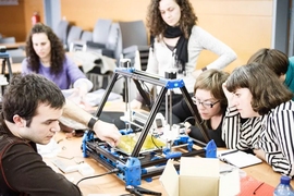
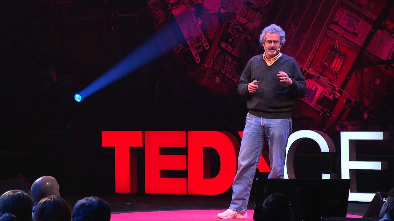
Ten years ago Neil Gershenfeld, professor of media arts and sciences and the founder and director of MIT’s Center for Bits and Atoms (CBA), began an outreach project that has grown into a global program for empowering local invention, engineering education, and entrepreneurship. He developed self-contained fabrication shops equipped with the latest rapid-prototyping equipment — laser cutters, computer-controlled milling machines, 3-D printers, and so on — that could be easily installed anywhere in the world. Since then, hundreds of what came to be called Fab Labs have been installed in dozens of countries, and last August thousands of the labs’ users and operators gathered at MIT for a 10th-anniversary conference. MIT News asked Gershenfeld to describe the growth and impact of this project.
Q: I understand that the core of the Fab Lab idea has to do with the concept of digital fabrication. Just what is digital fabrication?
A: The first computer-controlled milling machine was made at MIT in 1952. Since then, many kinds of end effectors — the part of a manufacturing machine that actually does the work — have been introduced, both adding material to an object and subtracting material from one. However, like the original Numerically Controlled (NC) mill, the physical processes used in today's most advanced rapid-prototyping tools still continuously add or remove material.
Around the time the first NC mill was being developed, Claude Shannon, the pioneer of information theory, was writing his seminal MIT master’s thesis. Digital computing and communications rest on threshold theorems, which show that by manipulating discrete symbols rather than continuous quantities, imperfect devices can operate more or less perfectly.
A third digital revolution is now underway that is extending this insight into fabrication, by discretizing not just the description of a design but also the materials that it is made from, in the same way that living systems are assembled from a small set of amino acids. Collaborative CBA projects are coding construction of systems ranging from molecular machines, to integrated electronics, to aircraft and space structures.
Q: Can you describe what a Fab Lab is?
A: CBA runs a digital fabrication research facility that was originally created with National Science Foundation support. That contains tools worth millions of dollars, with a research roadmap leading up to a Star Trek-style replicator. Fab Labs began as a modest outreach project for the NSF, to expand access to these capabilities. They unexpectedly spread into a global network, now approaching 1,000 labs.
A Fab Lab today fills a room, weighs about 2 tons, and costs about $100,000. That includes 3-D scanning and printing, large-format and precision machining, computer-controlled lasers and knives, surface-mount electronics production, embedded programming, and computing tools for design and collaboration. With these, it's possible to locally produce and customize products that are mass-produced today, such as consumer electronics and furniture.
There’s a very close analogy with the history of computing. The Internet was developed many years before the personal computer, on minicomputers that matched the size, cost, and complexity of a Fab Lab. The technologies were eventually integrated in a personal computer, but it wasn't necessary to wait for that to happen to develop their applications. Likewise, real personal fabricators are still many years off, but Fab Labs today emulate what they will eventually be able to do. Last summer we brought participants from 78 countries to MIT for FAB11, the annual meeting of the network. Highlights from it included the leadership of Boston, Somerville, and Cambridge, Massachusetts, joining Barcelona in a 40-year countdown to urban self-sufficiency; legislation in Congress to charter a National Fab Lab Network; and a pop-up lab that followed at the U.N. General Assembly.
Q: How does this all fit within the Institute? Digital computing is taught in computer science, digital communication in electrical engineering; how is digital fabrication taught?
A: To fill that gap I started teaching a rapid-prototyping class, How To Make (Almost) Anything (MAS.863). That was aimed at a small group of students doing this research, but it has been overwhelmed every year by hundreds of students wanting to take the class. To handle that demand we've expanded to include multiple shops at MIT, with more being planned, and now one of the sections is at Harvard for all the students cross-registering from there. What I enjoy most is how this crosses classroom boundaries, with students ranging from new undergrads to new faculty members, and with artists teaching engineers about engineering, and engineers teaching artists about art. There have also been interesting implications for Institute policy, such as being able to treat making on an equal footing as studying.
MIT’s fab class has spawned a global counterpart, the Fab Academy, which now encompasses 100 participating sites. It's a distributed rather than distance-learning model: Students with peers are organized in workgroups in Fab Labs, with local instructors and tools, which are then linked globally through interactive video lectures and collaborative project management. This platform is now being used for a second class in biotechnology, called How To Grow (almost) Anything, led by George Church. In what could be called “inreach” this started in the Fab Lab network but is now being taken by Harvard and MIT students.
This for me is the ultimate implication. MIT can fit a few thousand people, out of a planet of a few billion. Wherever we open a Fab Lab, we've found that it attracts exactly the same profile of bright, inventive people. The intersection of digital computing and communications with digital fabrication makes it possible to effectively bring the campus to them, thereby accessing more of the planet's brainpower.


