New findings from a team at MIT and other institutions could provide a pathway toward a kind of two-dimensional microchip that would make use of a characteristic of electrons other than their electrical charge, as in conventional electronics. The new approach is dubbed “valleytronics,” because it makes use of properties of an electron that can be depicted as a pair of deep valleys on a graph of their traits.
The findings are described in a paper appearing in the journal Nature Materials, co-authored by MIT graduate student Edbert Jarvis Sie, MIT associate professor Nuh Gedik, and five others.
The material the team studied is called tungsten disulfide (WS2), which belongs to a class of 2-D crystals known as transition metal dichalcogenides (TMDs). Like the single-layer carbon material called graphene, TMDs form thin films with a hexagonal, chicken-wire-like structure just a few atoms in thickness. (In the case of graphene, it is just a single atomic layer, while the TMDs are three atoms thick.)
Conventional electronics, including the microchips that power today’s computers, smartphones and tablets, manipulate charges carried by the electrons that flow through them. But other characteristics of the electrons could also be used to carry information: Their spin, for example, could lead to new “spintronic” devices.
Now valleytronics, another way of storing and manipulating data, could take a step toward practical applications through this latest research.
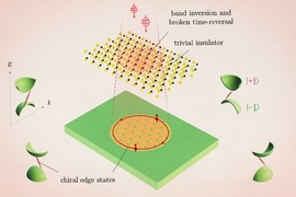
Valleytronics, which is a bit less intuitive to understand, has the potential to produce highly efficient devices, the team says. It is based on the fact that in certain materials, when the energy of electrons is plotted relative to their momentum on a graph, the resulting curve features two deep valleys. If subjected to certain perturbations, these two valleys can have unequal depth, giving the electrons a preference to populate one of the two valleys. The two different states can be used to represent the zeroes and ones of data.
“We discovered a way to directly control this valley by using light,” explains Sie, a PhD student in physics. And because of the two-dimensional nature of the material and its mechanical strength, valleytronics could be used to make flexible electronics, adds Gedik, the Biedenharn Career Development Associate Professor of Physics.
While tungsten disulfide could be used to create conventional charge-based electronic devices, or spintronic devices, it also has the properties needed, in theory, to create valleytronics, Gedik says.
On the chart of the energy of electrons in this material versus their momentum, “an electron cannot take any value it wants, it has to be on a specific curve, and that curve has two valleys,” he explains. Electrons naturally settle into the lowest-energy values available, but in this material that low point can be in either of the two valleys, since the electrons in the two valleys have equal energy. However, it is desirable to induce a difference in the energies of the electrons in the two valleys, since that difference can then be used to transfer information, Gedik says.
This much was already known, but attempts to shift the relative energies of the valleys have been limited to the idea of using magnetic fields. The problem is that the strength of the magnetic fields needed to achieve even a minuscule change in the valleys is far greater than can be achieved in an ordinary lab — hundreds of tesla.
The significant advance reported in this new research is that a much greater energy shift can be achieved with a relatively conventional laser pulse with a special polarization, providing a new method of control for valleytronic devices, the researchers say. In principle, Gedik says, it should now be possible to design devices in which all three properties of the electrons — charge, spin, and valleys — could be independently manipulated.
This work is just a beginning, Gedik says. Knowing that the effect works well in this material, the team hypothesized that it should also be possible to induce a new state of matter in this material using the same approach. “We want to actually experimentally observe this, and show that this new state exists,” he says.
David Hsieh, an assistant professor of physics at Caltech who was not connected to this research, says, “Being able to manipulate the valley degree of freedom in two-dimensional transition metal dichalcogenides would enable their application in the field of valleytronics. … This experiment makes a large step toward realizing this goal by demonstrating a method to control the energy difference between two valleys in tungsten disulfide for the first time.”
The research team also included MIT assistant professor of physics Liang Fu and associate professor of electrical engineering Jing Kong, graduate student James McIver of MIT and Harvard University, and assistant professor Yi-Hsien Lee of National Tsing-Hua University in Taiwan. The work was supported by the Department of Energy, the National Science Foundation, and the Ministry of Science and Technology of the Republic of China.


