Nanofibers — polymer filaments only a couple of hundred nanometers in diameter — have a huge range of potential applications, from solar cells to water filtration to fuel cells. But so far, their high cost of manufacture has relegated them to just a few niche industries.
In the latest issue of the journal Nanotechnology, MIT researchers describe a new technique for producing nanofibers that increases the rate of production fourfold while reducing energy consumption by more than 90 percent, holding out the prospect of cheap, efficient nanofiber production.
“We have demonstrated a systematic way to produce nanofibers through electrospinning that surpasses the state of the art,” says Luis Fernando Velásquez-García, a principal research scientist in MIT’s Microsystems Technology Laboratories, who led the new work. “But the way that it’s done opens a very interesting possibility. Our group and many other groups are working to push 3-D printing further, to make it possible to print components that transduce, that actuate, that exchange energy between different domains, like solar to electrical or mechanical. We have something that naturally fits into that picture. We have an array of emitters that can be thought of as a dot-matrix printer, where you would be able to individually control each emitter to print deposits of nanofibers.”
Tangled tale
Nanofibers are useful for any application that benefits from a high ratio of surface area to volume — solar cells, for instance, which try to maximize exposure to sunlight, or fuel cell electrodes, which catalyze reactions at their surfaces. Nanofibers can also yield materials that are permeable only at very small scales, like water filters, or that are remarkably tough for their weight, like body armor.
The standard technique for manufacturing nanofibers is called electrospinning, and it comes in two varieties. In the first, a polymer solution is pumped through a small nozzle, and then a strong electric field stretches it out. The process is slow, however, and the number of nozzles per unit area is limited by the size of the pump hydraulics.
The other approach is to apply a voltage between a rotating drum covered by metal cones and a collector electrode. The cones are dipped in a polymer solution, and the electric field causes the solution to travel to the top of the cones, where it’s emitted toward the electrode as a fiber. That approach is erratic, however, and produces fibers of uneven lengths; it also requires voltages as high as 100,000 volts.
Thinking small
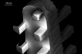
Velásquez-García and his co-authors — Philip Ponce de Leon, a former master’s student in mechanical engineering; Frances Hill, a former postdoc in Velásquez-García’s group who’s now at KLA-Tencor; and Eric Heubel, a current postdoc — adapt the second approach, but on a much smaller scale, using techniques common in the manufacture of microelectromechanical systems to produce dense arrays of tiny emitters. The emitters’ small size reduces the voltage necessary to drive them and allows more of them to be packed together, increasing production rate.
At the same time, a nubbly texture etched into the emitters’ sides regulates the rate at which fluid flows toward their tips, yielding uniform fibers even at high manufacturing rates. “We did all kinds of experiments, and all of them show that the emission is uniform,” Velásquez-García says.
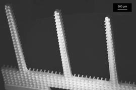
To build their emitters, Velásquez-García and his colleagues use a technique called deep reactive-ion etching. On either face of a silicon wafer, they etch dense arrays of tiny rectangular columns — tens of micrometers across — which will regulate the flow of fluid up the sides of the emitters. Then they cut sawtooth patterns out of the wafer. The sawteeth are mounted vertically, and their bases are immersed in a solution of deionized water, ethanol, and a dissolved polymer.
When an electrode is mounted opposite the sawteeth and a voltage applied between them, the water-ethanol mixture streams upward, dragging chains of polymer with it. The water and ethanol quickly dissolve, leaving a tangle of polymer filaments opposite each emitter, on the electrode.
The researchers were able to pack 225 emitters, several millimeters long, on a square chip about 35 millimeters on a side. At the relatively low voltage of 8,000 volts, that device yielded four times as much fiber per unit area as the best commercial electrospinning devices.
The work is “an elegant and creative way of demonstrating the strong capability of traditional MEMS [microelectromechanical-systems] fabrication processes toward parallel nanomanufacturing,” says Reza Ghodssi, a professor of electrical engineering at the University of Maryland. Relative to other approaches, he adds, there is “an increased potential to scale it up while maintaining the integrity and accuracy by which the processing method is applied.”


