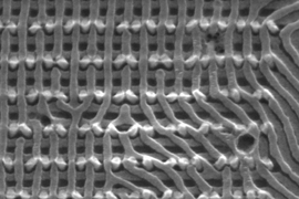
Although similar self-assembling structures with very fine wires have been produced before, this is the first time the structures have been extended into three dimensions with different, independent configurations on different layers, the researchers say. The research is published this week in the journal Science.
Caroline Ross, the Toyota Professor of Materials Science and Engineering at MIT, says there has been “a lot of interest” among semiconductor researchers in finding ways to produce chip features that are much narrower than the wavelength of light — and hence narrower than what can be achieved using present light-based fabrication systems. Self-assembly based on polymers has been an active area of research, Ross says, but “what we did in this paper was push it into the third dimension.”
She and her colleagues began by creating an array of tiny posts on a substrate of silicon; they then coated the surface with materials called block copolymers, which have a natural tendency to assemble into long cylindrical structures. By carefully controlling the initial spacing of the posts, Ross explains, the researchers were able to set the spacing, angles, bends and junctions of the cylinders that form on the surface. What’s more, she says, “Each of the two layers of cylinders can be independently controlled using these posts,” making it possible to create complex 3-D configurations.
Amir Tavakkoli, a visiting graduate student from the National University of Singapore and lead author of the Science paper, says many researchers have tried to produce complex arrangements of nanoscale wires through self-assembly. But earlier attempts used complex processes with many steps, and had failed to control the resulting configurations well. The new system is simpler, Tavakkoli says, and “not only controlled the alignment of the wires, but showed we can even have sharp bends and junctions” at precisely determined locations.
“It wasn’t expected to be possible,” says MIT graduate student Kevin Gotrik. “It was a surprising result. We stumbled upon it, and then had to figure out how it works.”
There were a number of barriers to overcome in making the system practical, Gotrik says. For example, the posts fabricated on the surface are the key to controlling the whole self-assembly process, but they need to be quite a bit taller than they are wide, which could lead some to topple over; the MIT team ultimately found materials and shapes that would be stable. “We explored a wide range of conditions,” Gotrik says.
Graduate student Adam Hannon says the team used computer simulations of the structures in order to explore the effects of different post configurations on the double-layer 3-D structure. These simulations were compared with the most promising structures observed in the laboratory to get greater insight into how to control the resulting structures that formed.
So far, the MIT team has only produced two-layer configurations, but Alfredo Alexander-Katz, an assistant professor of materials science and engineering, says, “I think it would be feasible to go to three layers” while still maintaining full control over the arrangement of structures on each layer.
A key enabling technology was the MIT lab’s capability, using electron-beam lithography, to make 10-nanometer-wide cylindrical posts with precisely controlled positioning. These posts, in turn, guide the positioning of the self-assembling cylinders. Karl Berggren, an associate professor of electrical engineering, says it’s as if the lithography puts down an array of pillars, and these pillars then control the complex, multilevel routing of crisscrossing highways.
In earlier work, the MIT researchers had demonstrated that this self-assembly method could be used to create wires that are much finer than those that can be made by existing photolithography techniques for producing microchips — and thus help lead the way to next-generation devices that pack even more wires and transistors into a given area of silicon chip material. “In principle, this is scalable to quite small dimensions,” Ross says, far smaller than the 15-nanometer width of the cylinders produced so far — which is already less than half the width of the finest wires in existing microchips.
The basic technologies involved are compatible with existing manufacturing equipment in the semiconductor industry, the researchers say. But this is basic research that is probably still far from actual chip production, they caution. Within the next year the team hopes to use this methodology to produce a simple electronic device.
The technique is not limited to producing wires on a silicon chip, Ross and her colleagues say. The same method could be used to create 3-D arrays of other kinds of materials — such as proteins or DNA molecules, for example — in order to create biological detectors or drug-delivery systems.
Craig Hawker, a professor of chemistry and biochemistry at the University of California at Santa Barbara, says this is a “far-reaching finding,” which “goes a long way to fulfilling the demands of the International Technology Roadmap for Semiconductors, which calls for a robust, commercially viable nanopatterning technique.”
Hawker adds, “The robustness and power of this approach may also lead to applications outside lithography and microelectronics, with impact in water purification, membranes and organic photovoltaics.” He says this work is “a spectacular example of multidisciplinary work, with advances in chemistry, physics and nanotechnology seamlessly combined to address a critical technological and important societal problem.”
The work was supported by the Semiconductor Research Corporation, the FENA Center, the Nanoelectronics Research Initiative, the Singapore-MIT Alliance, the National Science Foundation, Tokyo Electron and Taiwan Semiconductor Manufacturing Company.


