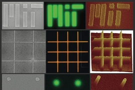
The size of a semiconductor nanocrystal determines its electrical and optical properties. But it’s very hard to control the placement of nanocrystals on a surface in order to make structurally uniform films. Typical nanocrystal films also have cracks that limit their usefulness and make it impossible to measure the fundamental properties of these materials.
Now, researchers at MIT say they have found ways of making defect-free patterns of nanocrystal films where the shape and position of the films are controlled with nanoscale resolution, potentially opening up a significant area for research and possible new applications.
“We’ve been trying to understand how electrons move in arrays of these nanocrystals,” which has been difficult with limited control over the formation of the arrays, says physicist Marc Kastner, the Donner Professor of Science, dean of MIT’s School of Science and senior author of a paper published online in the journal Nano Letters.
The work builds on research by Moungi Bawendi, the Lester Wolfe Professor of Chemistry at MIT and a co-author of this paper, who was one of the first researchers to precisely control nanocrystal production. Such control made it possible, among other things, to produce materials that glow, or fluoresce, in a range of different colors based on their sizes — even though they are all made of the same material.
In the initial phases of the new work, postdoc Tamar Mentzel produced nanoscale patterns that emit invisible infrared light. But working on such systems is tedious, since each fine-tuning has to be checked using time-consuming electron microscopy. So when Mentzel succeeded in getting semiconductor nanocrystal patterns to glow with visible light, making them visible through an optical microscope, it meant that the team could greatly speed the development of the new technology. “Even though the nanoscale patterns are below the resolution limit of the optical microscope, the nanocrystals act as a light source, rendering them visible,” Mentzel says.
The electrical conductivity of the researchers’ defect-free films is roughly 180 times greater than that of the cracked films made by conventional methods. In addition, the process developed by the MIT team has already made it possible to create patterns on a silicon surface that are just 30 nanometers across — about the size of the finest features possible with present manufacturing techniques.
The process is unique in producing such tiny patterns of defect-free films, Mentzel says. “The trick was to get the film to be uniform, and to stick” to the silicon dioxide substrate, Kastner adds. That was achieved by leaving a thin layer of polymer to coat the surface before depositing the layer of nanocrystals on top of it. The researchers conjecture that tiny organic molecules on the surface of the nanocrystals help them bind to the polymer layer.
Such nanocrystal patterns could have many applications, Kastner says. Because these nanocrystals can be tuned not only to emit but also to absorb a wide spectrum of colors of light, they could enable a new kind of broad-spectrum solar cell, he says.
But Kastner and Mentzel’s personal interest has more to do with basic physics: Since the minuscule crystals behave almost like oversized atoms, the researchers aim to use the arrays to study fundamental processes of solids, Mentzel says. The success of this technique has already enabled new research on how electrons move in the films.
Such materials could also be used to develop sensitive detectors for tiny amounts of certain biological molecules, either as screening systems for toxins or as medical testing devices, the researchers say.
Douglas Natelson, a professor of physics and astronomy at Rice University who was not involved in this work, says, “The challenge in the past has been achieving thin, uniform films, patterned at high resolution, with good contact between the nanocrystals and no cracking.” The MIT team’s approach, he says, “while deceptively simple in appearance, accomplishes all of these objectives.”
Natelson adds: “I think this is a very nice achievement. The fluorescence images showing the nanopatterned films are eye-popping, particularly for those who know how tough this is.”
The research was supported by the U.S Army Research Office, the Department of Energy and Samsung.


